- 您现在的位置:买卖IC网 > Sheet目录1234 > NP1500SCT3G (ON Semiconductor)THYRISTOR TSPD 100A 150V SMB
�� �
�
�NCP1500�
�PWM� Section�
�The� PWM� section� consists� of� a� PWM� comparator,� set�
�dominant� latch,� slope� compensation� circuit,� current� sense�
�circuit,� and� current� limit� circuit.�
�The� NCP1500� operates� as� a� current� mode� regulator� in�
�PWM� mode.� In� this� mode,� a� PWM� pulse� from� the�
�synchronization� section� initiates� the� output� switch�
�conduction.� Output� switch� conduction� is� terminated� when� the�
�peak� inductor� current� reaches� a� threshold� level� established� by�
�the� error� amplifier.� The� output� switch� conduction� duty� cycle�
�is� allowed� to� go� to� 100%� to� increase� transient� load� response�
�when� going� from� light� load� to� heavy� load.�
�A� reset� dominant� latch� is� provided� in� the� NCP1500.� A� 3�
�input� OR� gate� controls� the� reset� pin.� Any� one� of� the� 3� inputs�
�will� terminate� output� switch� conduction.� Once� terminated,�
�output� switch� conduction� cannot� begin� again� until� the� next�
�PWM� pulse.� The� only� state� the� NCP1500� does� not� switch�
�every� cycle� is� if� the� 5%� overvoltage� comparator� trips.� When�
�the� comparator� trips,� the� switching� regulator� will� remain� off�
�until� the� voltage� drops� below� the� nominal� voltage.� This� state�
�is� similar� to� a� PFM� mode� of� operation.� Output� switch�
�conduction� can� begin� at� the� next� PWM� cycle� after� the� OVP�
�input� is� reset.�
�Current� mode� controllers� can� exhibit� an� instability� at� duty�
�cycles� over� 50%.� A� slope� compensation� circuit� is� provided�
�inside� the� NCP1500� to� overcome� the� potential� instability.�
�Slope� compensation� consists� of� a� ramp� signal� generated� by�
�the� synchronization� block� and� adding� this� to� the� current�
�signal.� The� summed� signal� is� then� applied� to� the� PWM�
�comparator.�
�A� current� limit� feature� is� provided� in� the� PWM� mode� only.�
�The� current� limit� is� set� to� allow� peak� switch� current� in� excess�
�of� 800� mA.� It� is� implemented� as� a� cycle� ?� by� ?� cycle� current�
�limit.� Each� on� ?� cycle� is� treated� as� a� separate� situation.�
�Current� limiting� is� implemented� by� monitoring� the� output�
�switch� transistor� current� buildup� during� conduction.� An�
�error� signal� is� generated� upon� sensing� an� over� ?� current�
�condition.� This� signal� is� subtracted� from� the� error� amplifier�
�output.� This� in� turn� reduces� the� PWM� comparison� threshold�
�voltage,� thus� limiting� the� output� duty� cycle.�
�3.6040�
�3.6000�
�3.5960�
�400� m�
�200� m�
�0.00�
�400� m�
�300� m�
�200� m�
�400� m�
�100� m�
�?� 200� m�
�1.01�
�1.00�
�990� m�
�3.70�
�1.35�
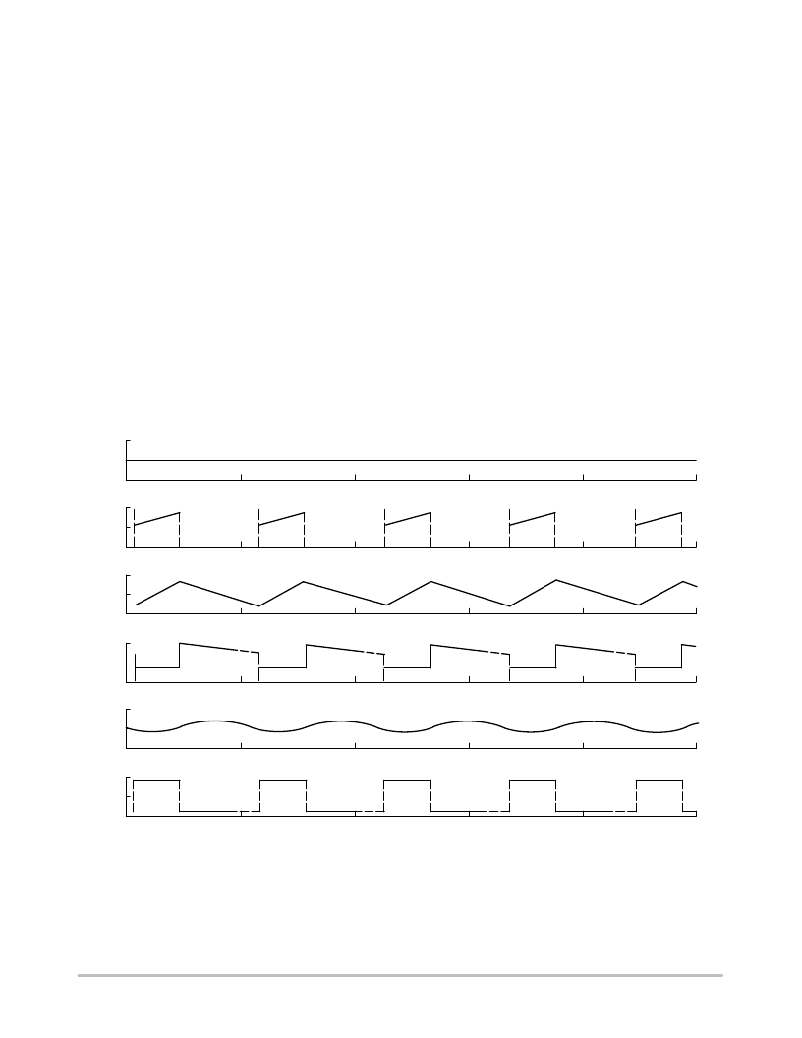
�V� IN�
�I� FET�
�I� L�
�I� diode�
�V� O�
�V� LX�
�?� 1.00�
�198.0�
�201.0�
�204.0�
�207.0�
�210.0�
�213.0�
�TIME� (� m� )�
�Figure� 4.� PWM� Waveforms� During� Normal� Operation�
�http://onsemi.com�
�6�
�发布紧急采购,3分钟左右您将得到回复。
相关PDF资料
NP2600SCMCT3G
IC TSPD SURGE DEVICE 150MA SMB
NP3100SBMCT3G
IC TSPD SURGE PROTECT 80A SMB
NP3500SCT3G
IC THY SURGE PROTECTOR 350V SMB
NPB02DVFN-RC
CONN JUMPER SHORTING 1.27MM GOLD
NPB02SVAN-RC
CONN JUMPER SHORTING 1.27MM GOLD
NPB02SVFN-RC
CONN JUMPER SHORTING 1.27MM GOLD
NPC02SXNN-RC
CONN JUMPER SHORTING .100" GOLD
NPC02SXON-RC
CONN JUMPER SHORTING .100" GOLD
相关代理商/技术参数
NP1500SDMCT3G
制造商:ONSEMI 制造商全称:ON Semiconductor 功能描述:High Current TSPD
NP1500U
制造商:ORION POWER SYSTEMS, INC. 功能描述:UPS; Network Pro 1500 Line Interactive; Rated at 1500 VA and 1300 Watts
NP15P04SLG-E1-AY
功能描述:MOSFET P-CH -40V MP-3ZK/TO-252 RoHS:是 类别:分离式半导体产品 >> FET - 单 系列:- 标准包装:1,000 系列:MESH OVERLAY™ FET 型:MOSFET N 通道,金属氧化物 FET 特点:逻辑电平门 漏极至源极电压(Vdss):200V 电流 - 连续漏极(Id) @ 25° C:18A 开态Rds(最大)@ Id, Vgs @ 25° C:180 毫欧 @ 9A,10V Id 时的 Vgs(th)(最大):4V @ 250µA 闸电荷(Qg) @ Vgs:72nC @ 10V 输入电容 (Ciss) @ Vds:1560pF @ 25V 功率 - 最大:40W 安装类型:通孔 封装/外壳:TO-220-3 整包 供应商设备封装:TO-220FP 包装:管件
NP15P06SLG-E1-AY
功能描述:MOSFET P-CH -60V MP-3ZK/TO-252 RoHS:是 类别:分离式半导体产品 >> FET - 单 系列:- 标准包装:1,000 系列:MESH OVERLAY™ FET 型:MOSFET N 通道,金属氧化物 FET 特点:逻辑电平门 漏极至源极电压(Vdss):200V 电流 - 连续漏极(Id) @ 25° C:18A 开态Rds(最大)@ Id, Vgs @ 25° C:180 毫欧 @ 9A,10V Id 时的 Vgs(th)(最大):4V @ 250µA 闸电荷(Qg) @ Vgs:72nC @ 10V 输入电容 (Ciss) @ Vds:1560pF @ 25V 功率 - 最大:40W 安装类型:通孔 封装/外壳:TO-220-3 整包 供应商设备封装:TO-220FP 包装:管件
NP15P06SLG-E2-AY
制造商:Renesas Electronics Corporation 功能描述:
NP16
制造商:未知厂家 制造商全称:未知厂家 功能描述:16 AMPERE SILICON RECTIFIER
NP1-6
制造商:Dantona Industries 功能描述:ENERSYS NP1-6 6 VOLT SEALED LEAD ACID BATTERY 制造商:YUASA 功能描述:BATTERY 6V 1AH 制造商:Yuasa Battery Inc 功能描述:BATTERY, 6V, 1AH
NP160CR832K12E
制造商:NYLOK 功能描述: